Signal Integrity Essentials for Next Generation Systems

Overview

Signal integrity has been around for a few decades and it has matured into a discipline that many may think does not hold any new surprises.

On the contrary, people actively working in the field find new challenges and revelations on a daily basis; not because the underlying physics has changed, but because the increasing data rates and larger, higher-power chips require us to take into account effects that did not matter in the past.

This newly updated and expanded course summarises some of the most important and often counter-intuitive aspects of signal integrity that are a MUST for all engineers whether they work at relatively low speed or on cutting-edge signalling with 200Gb/s speed and beyond.

Each major topic starts with a brief overview of the basics, followed by a unique blend of live measurements and simulations to illustrate challenges, constraints, limitations and available solutions.

This course is taught by a practitioner of high-speed electronics with many years of successful design experience as well as decades of teaching in academia. You will learn the important fundamentals of the subject as well as little-known tricks to enhance your knowledge.

Programme details

Day 1:

  • Introduction: why SI engineers also need to know the basics of PI and EMC. Illustrations of how these disciplines can interact in unexpected ways in our modern designs.
  • Impedance, reflections, matching: after a brief summary of reflections, transmissions and S parameters, we discuss how much reflection is too much for the different applications and look at the effects of anisotropy, as well as the untold perils of periodicity created by glass weave, BGA and connector perforations and backplane slots.
  • PCB and cable constructions: what we don’t know about the materials and processes can hurt our design. Stackup nuances that matter for signal integrity: which layer is core vs. prepeg matters a lot under some circumstances. Why knowing the laminate parameters alone is not enough to determine losses; how the manufacturing processes influence the resulting behaviour.
  • Discontinuities: how different types of vias influence signal integrity: blind vias, skip vias, buried vias, HDI and UHDI construction. When and why do you need to worry about bends; the full picture. How to optimise via transitions and when this matters.

Day 2:

  • Everything you need to know about losses: absorption, reflection, radiation. Dielectric vs. conductor losses. Effect of surface roughness, glass weave, etch variation. Effect of temperature and humidity on conductive and dielectric losses.
  • Crosstalk: The hidden far-end crosstalk in striplines. Ways to reduce far end crosstalk in microstrip with tabbed traces. How a very important power distribution measurement principle applies to crosstalk measurements as well and what happens if we ignore it.
  • Differential signalling: comparing the performance of loosely and tightly coupled traces. Potential problems and solutions for delay-meander traces. Impact of reflections on skew. When, why and how skew can hurt your design.
  • System SI and material properties and process details: sources of anisotropy in laminates, impact of surface finish on signal integrity.

Day 3:

  • SI measurements: we need to know where the calibration's reference plane is. Comparison of major calibration options, how to choose among them. Which view is better for SI: frequency-domain VNA results or time-domain TDR data. Comparing pros and cons, reviewing cabling and SI probing options. Testing for environmental effects: impact of temperature and humidity.
  • Important rules to keep in mind for simulations. Simple and tricky pitfalls to avoid in selecting, creating and validating models. Which type of solver is best for a particular application? The challenges of and helpful suggestions for correlations related to port type, model size, sweep and convergence settings. Modelling temperature effects, roughness, dielectric loss. Mixed dielectrics, reliability and life expectancy of components. Explaining and analysing nuances of laminate material and component data sheets to which we must pay attention.

Attending Your Course 

Further details will be emailed to you two weeks ahead of your course, which will include registration information. 

Please get in touch if you have not received this information within five working days of the course start date.  

In the meantime, you may wish to plan your travel: Travel information

Digital Certification

In order to be eligible for a certificate of attendance, you will need to attend the whole course. Participants who meet this criterion will be emailed after the end of the course with a link, and instructions on how to access their University of Oxford digital certificate. 

The certificate will show your name, the course title and the dates of the course you attended. You will be able to download your certificate, as well as share it on social media if you choose to do so.

Fees

Description Costs
Course fee £1675.00
Discount package (with Power Distribution Design course) £3125.00

Payment

This course may be taken alongside Making Successful Power Distribution Designs for the AI Age for a discounted combined fee of £3,125. If you would like to opt for this, please select the relevant option after pressing 'Book Now'.

Fees include course materials, tuition, refreshments and lunches. The price does not include accommodation.

All courses are VAT exempt.

Register immediately online 

Click the “book now” button on this webpage. Payment by credit or debit card is required.

Request an invoice

If you require an invoice for your company or organisation, please email us to request an online enrolment form.

Tutor

Dr Istvan Novak

Course Tutor

Principal Signal and Power Integrity Engineer

Samtec

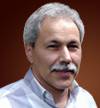
Istvan is the Principal Signal and Power Integrity Engineer at Samtec. He is currently working on new technologies and system designs that enable customers to improve power delivery and increase data speeds beyond 100Gbps. He is a Life Fellow of IEEE for his contributions to signal-integrity and power-integrity designs, modelling, measurements and simulations. He has 40+ years of experience in high-speed and high-power electronics designs as well as teaching and consulting.

Previously, Dr Novak was at Oracle/SUN for 21 years, working on new advanced power distribution design, signal integrity and validation methodologies. He was responsible for the power distribution and high-speed signal integrity designs of SUN's successful workgroup server families. He introduced the industry's first 25um power-ground laminates for large rigid computer boards, and worked with component vendors to create a series of low-inductance and controlled-ESR bypass capacitors.

Dr Novak also served as SUN's representative on the Copper Cable and Connector Workgroup of InfiniBand, and is engaged in the methodologies, designs and characterisation of power-distribution networks and CPU packages. He has twenty-five patents.

He is the lead author of Frequency-Domain Characterization of Power Distribution Networks (Artech House, 2007) and executive editor of Power Distribution Network Design Methodologies (IEC, 2008).

In 2020, Dr Novak was announced as Engineer of the Year at the DesignCon event in Santa Clara, Calif. (Jan 30, 2020).

For additional insight into Dr Novak, please read the EDN Network's Profile in Design.

Application

If you would like to discuss your application or any part of the application process before applying, please click Contact Us at the top of this page.

Level and demands

This course is intended for:

  • Board design engineers, system designers and signal-integrity specialists in the high-speed computing, networking and artificial intelligence, automotive, medical and defence industries, who are interested in a broader and better understanding of potential signal integrity issues.
  • Managers and engineers who need a better and deeper understanding of the simulation and measurement challenges and solutions in signal integrity.

Partcipants are expected to have a basic understanding of electronic circuits and waves.

Accommodation

Although not included in the course fee, accommodation may be available at our on-site Rewley House Residential Centre. All bedrooms are en suite and decorated to a high standard, and come with tea- and coffee-making facilities, free Wi-Fi access and Freeview TV. Guests can take advantage of the excellent dining facilities and common room bar, where they may relax and network with others on the programme.

To check prices, availability and to book rooms please visit the Rewley House Residential Centre website. 

Enrolled students are entitled to discounted accommodation rates for the purpose of study, at Rewley House, and can contact the administration team for the promotional code to use for making online accommodation bookings via the website.